This blogpost is longer than what I usually write about my projects, mainly because this project also became much bigger than anticipated in the beginning.
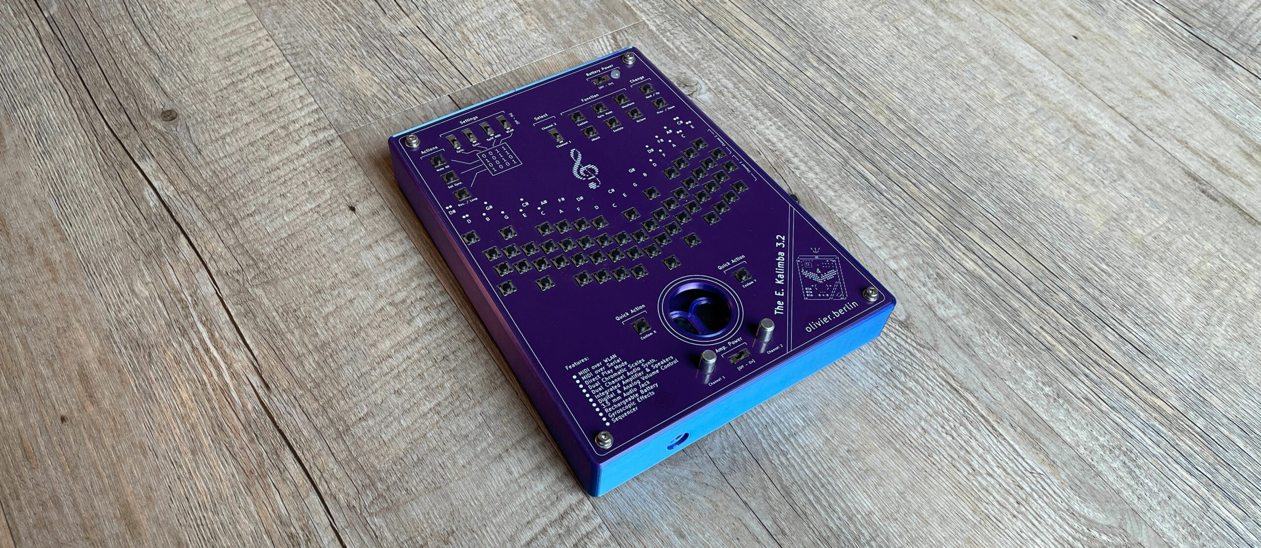
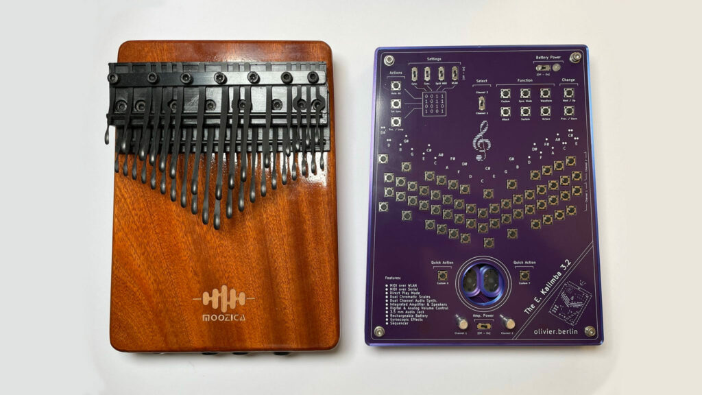
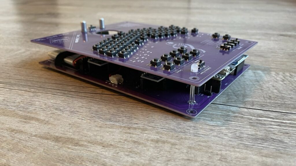
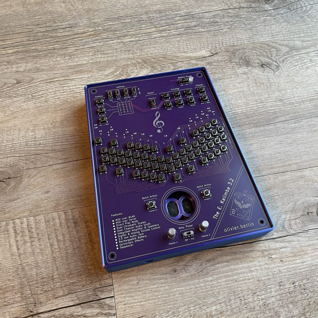
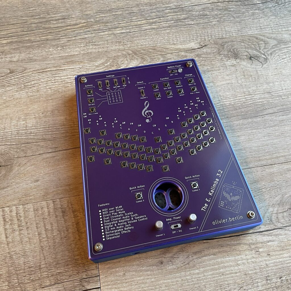
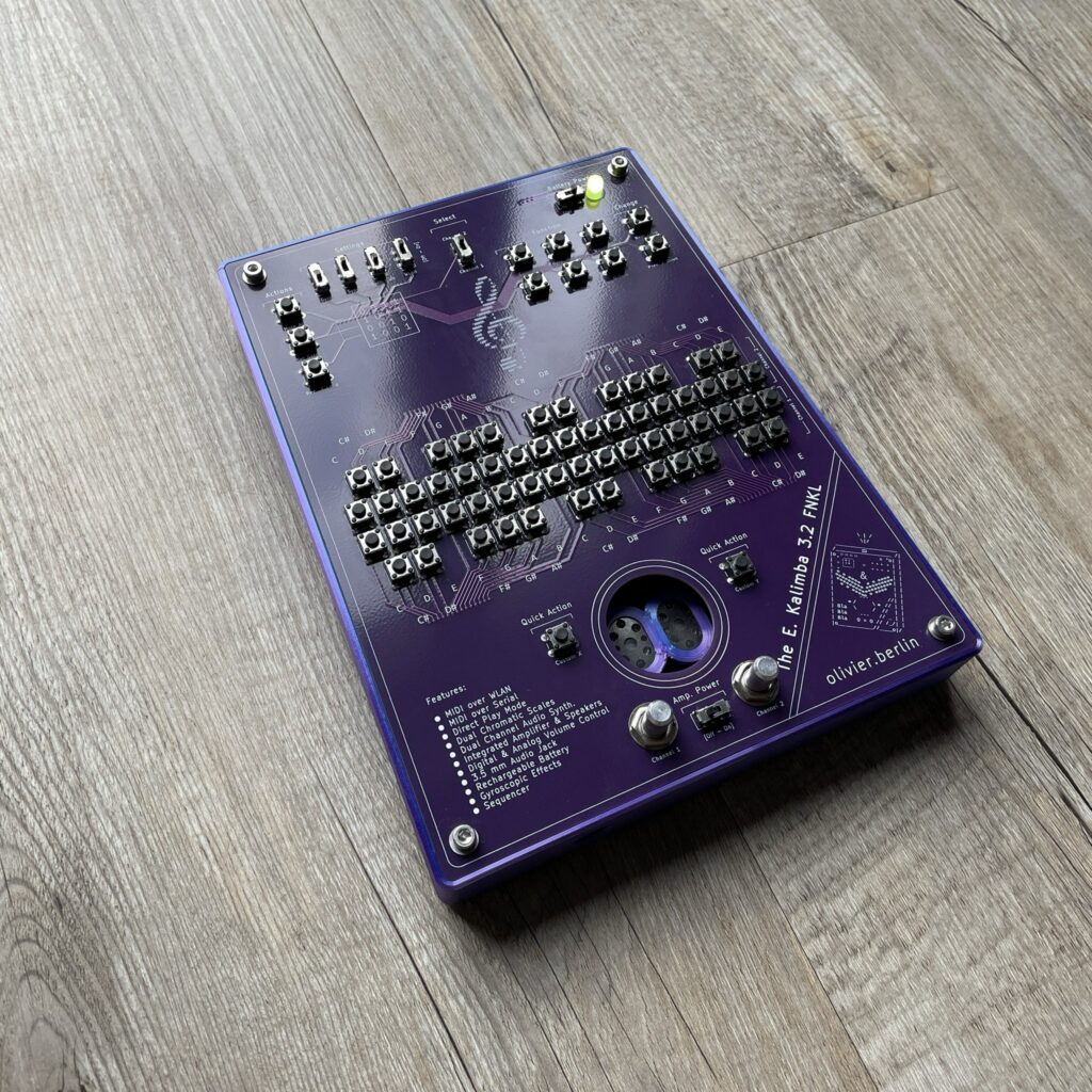
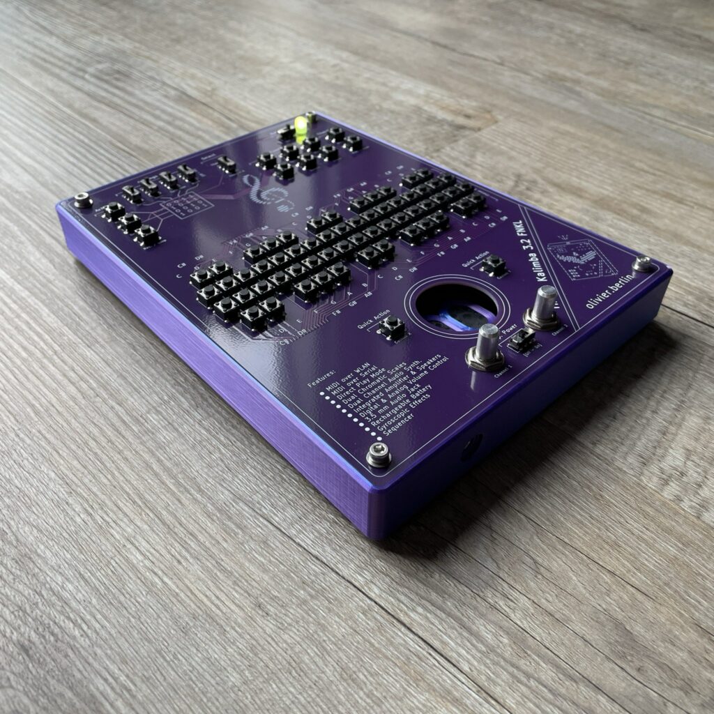
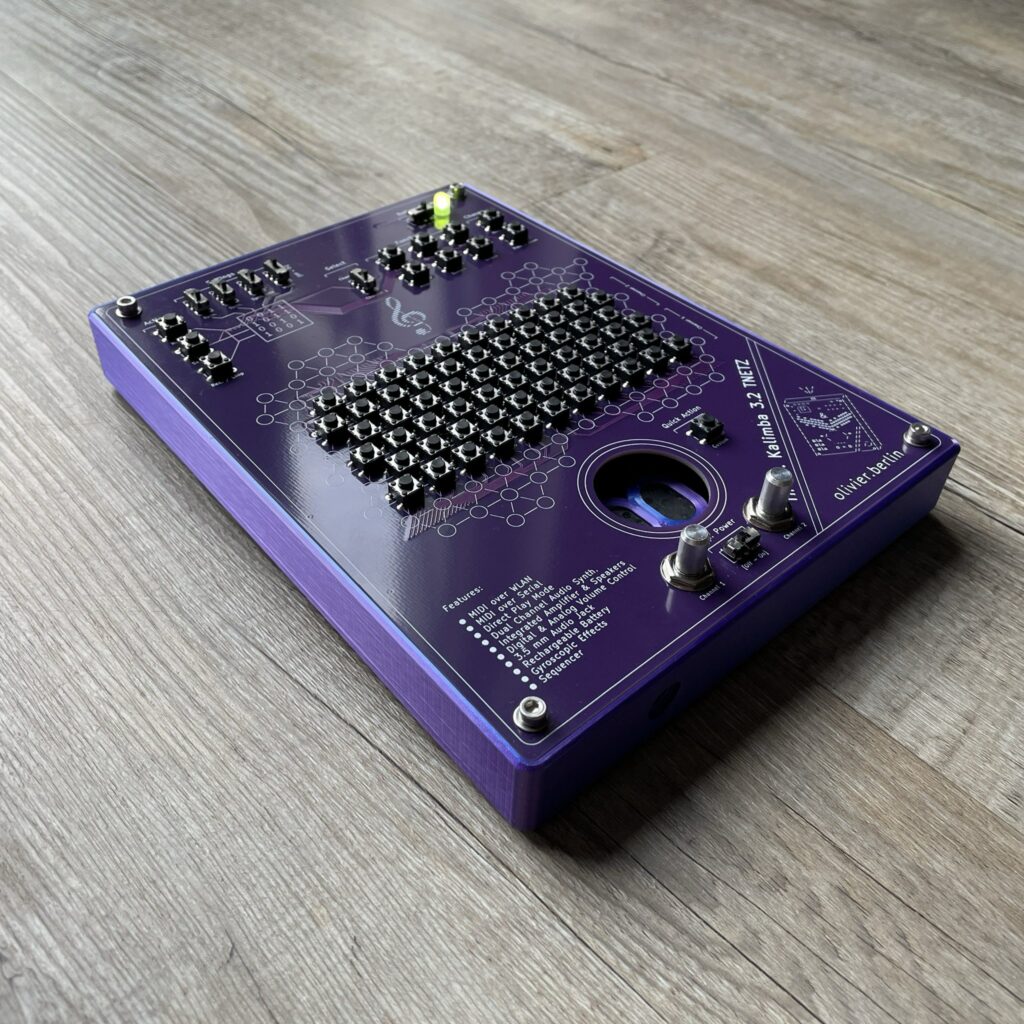
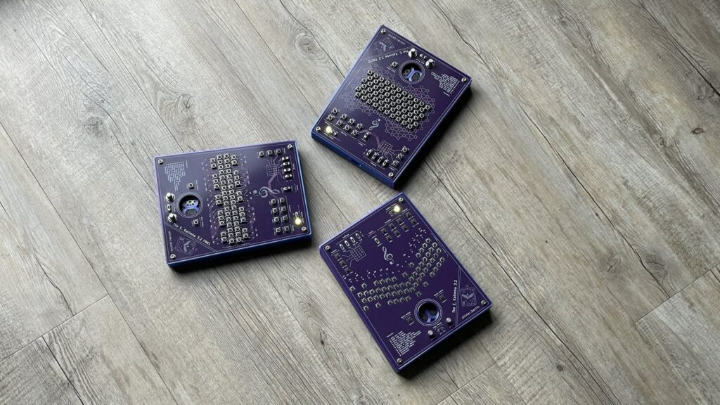
The TL;DR is a 100% custom, handheld, battery powered MIDI controller / synthesizer constructed from two custom PCBs stacked together. The device supports MIDI over serial as well as MIDI over WLAN but is also capable of playing back generated audio waves either using its onboard speakers or on an external audio device via its 3.5 mm audio jack, to make the need for a computer entirely optional. The top PCB is easily interchangeable and can have all sorts of different key layouts.
The whole project is open source using the MIT license and uses only standard off the shelf components. Everything is easily hand solderable and component cost is below 100 € (including the cost of the PCBs!), for a device that is packed with functionalities.
Main Features
- 2 * 29 tactile switches for notes
- 2 chromatic channels
- MIDI over WLAN
- MIDI over Serial
- Gyroscope for effects
- Dual on board audio generation
- Dual volume control
- 10 Buttons and 6 switches for different modes
- Integrated lipo battery
- Status LED for battery and to display modes
Story
Currently, the project is more or less concluded. I am happy with the overall state and the microcontroller is almost out of free program memory. The following paragraphs describe the journey to lead me to this point.
Version 1
After starting a new hobby (PCB design) at the end of 2024, I was looking for a new project where I could use this new skill. Some time ago, I built an electronic guitar. I always wanted to update this project with professionally manufactured PCB’s. But rather than reiterating on a finished project, I thought I should build something new.
Since Corona, I am in love with Kalimbas, and I always searched for a way to capture played Kalimba notes accurately on my PC. The best shot so far was a tool in Unity I developed that is capable of analyzing an audio source for peaks on different bands. This however only worked with 98% accuracy, even when the player played very consistently.
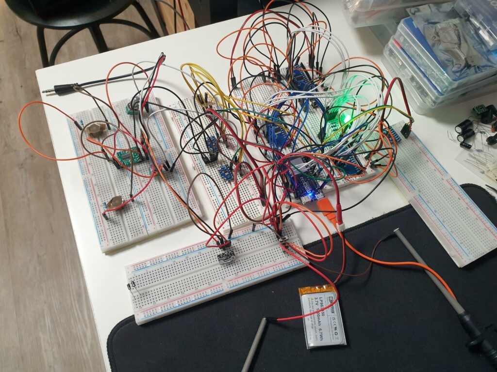
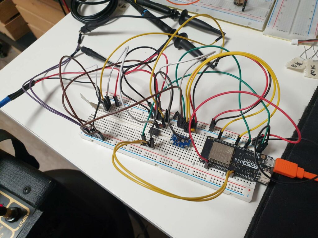
As my new project, I therefore figured I could build a true MIDI Kalimba. First, I measured my Kalimbas and the spacing between their notes and found out that the same buttons I used for my electronic guitar project would also be perfect for this application. This time however, I did not want to use multiple microcontrollers for the project and decided to test out multiplexers and their delays. On the breadboard, no delays were noticeable and hence I got to work with my new favorite open source tool KiCad. The project was supposed to be a quick weekend project so I focused on not adding any non essential features to my list of requirements. Only a microcontroller, one switch to trigger each note and one switch to mute that same note again.
Indeed, the design was ready to be ordered after only two evenings. The total cost including shipping was only 25 € (which I still think is crazy). And only a few days after, I held my new PCBs in my hands.
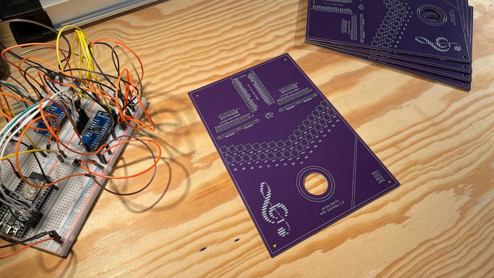
While waiting for delivery, I already started coding the firmware for the microcontroller. The soldering was easy and after plugging the instrument into my PC, I was pleased to see that all the buttons were working, although not in the correct order. I figured I had to fix up a few addresses but apart from that the project worked flawlessly out of the box.
In the upcoming days, this thing was my new fidget toy. It was hooked up to my PC at all times, and I regularly grabbed it when I felt like procrastinating on another project and played away. I was extremely happy with the look and feel and thought this thing was almost perfect.
Here is a short video showcasing the version 1.0 in its assembled state:
Version 2
However, I was slightly displeased with the arrangement of the switches. The horizontal spacing I used was a little too wide compared to a real Kalimba, but mostly the gap between the upper row and lower row was too large. My initial idea, that I could use one row to trigger notes and one row to mute notes, felt extremely unnatural to play but the second row proved to be nice to have another octave of notes at hand. Therefore, I did not want to get rid of the upper row, I only moved the buttons horizontally closer together. Another detail that I found slightly annoying on the V1 was that it needed my PC to be on and my digital audio workstation (DAW) to be open to produce sounds. What I enjoy most about real Kalimbas is their simplicity. They can easily be grabbed, played for a minute and put aside again. Since I was missing this a lot, I included on board audio generation to my list of desired features.
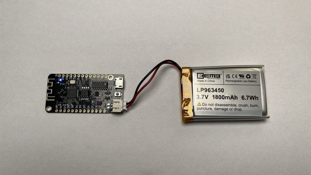
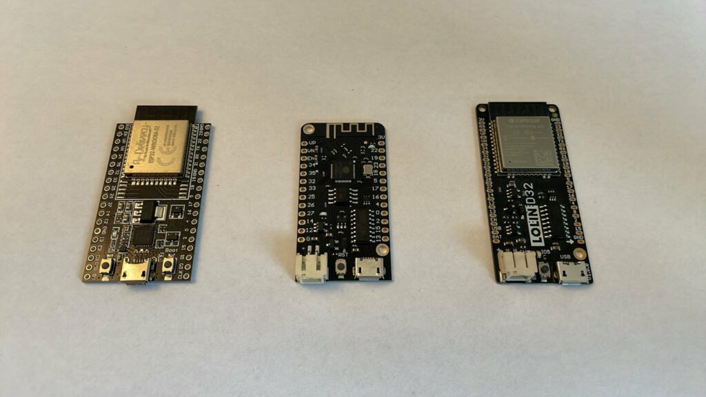
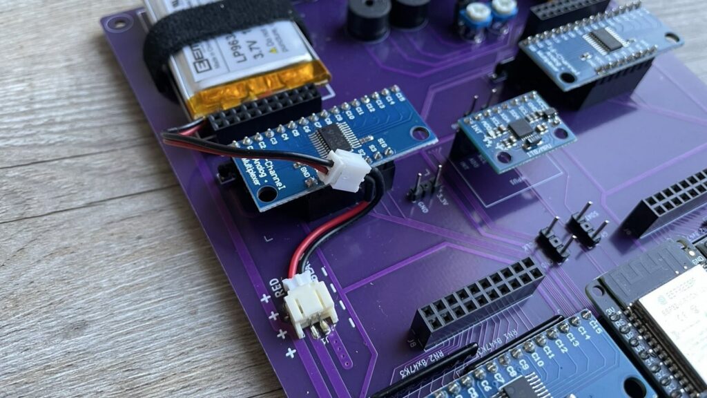
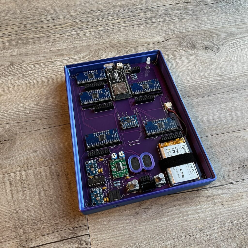
When basic audio generation was working on my breadboard, the PC was merely delivering power. It was obvious that I needed a portable energy source to achieve a truly standalone instrument. I looked into different ways of powering microcontrollers and concluded after many dead ends that my best bet would be a microcontroller with an already integrated charging circuit and a battery connector. This would also have the benefit that I would not block the USB port of the microcontroller. I therefore ditched the “ESP32 Board Dev Kit C V4” and switched to the “LOLIN32 Lite Board”, which would also free up a lot of space on the PCB.
But while being powered via battery, I had new issues with the audio amplifier not getting enough power from the microcontroller’s 3V3 pin. It could just not provide enough current and I would get frequent brown outs and clicking sounds from the resetting amp. This was a hard problem to solve. I tried multiple transistors and mosfets but all test setups proved to be too complicated or inefficient. In a stroke of luck, I stumbled over “ideal diodes modules”.
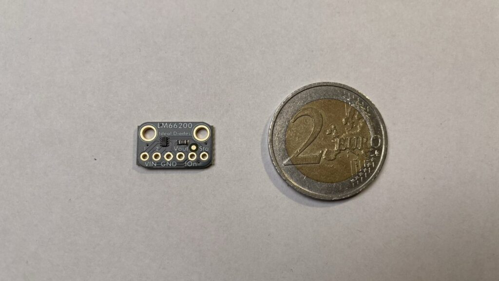
They can select a power source based on higher voltage. That was exactly what I needed. Now I could connect the audio amplifier to the USB power and the battery at the same time through this module. When the microcontroller is connected via USB, the USB is providing 5 V allowing the audio amplifier to draw current from the USB. If the microcontroller is not powered via USB, the USB is at 0V and the ideal diode module connects the battery to the amplifier directly. However, the “LOLIN32 Lite Board” did not give me access to the USB’s 5V pin, and I had to connect the battery to the microcontroller and could not connect the battery directly via a PCB trace. While searching for a solution and in the next stroke of luck, I stumbled over the LOLIN32 Lite Board’s bigger brother, the LOLIN D32. It had a battery pin that as well as a VUSB pin, directly connected to the USBs powerline. I ordered this chip and changed my microcontroller one more time.
Something entirely different that I found annoying after playing the V1 was that it was inconvenient to reflash the microcontroller each time I wanted to play with different octaves / wave forms. Therefore, I added dedicated switches and buttons to the design to have a way to select different modes.
When I was happy with the new design, I uploaded it to JLCPCB again and was about to press order. I decided not to go ahead immediately, but I had the idea to print out the PCB layout on paper and place all the components to check if they fit physically on the board. Then it struck me. When I changed to the last microcontroller board, I forgot to set the correct exclusion zone, and components were therefore overlapping. This was unfortunate. I added so many cool features to my project that I completely filled up all the usable space on my PCB. Also, I did not want to increase the size of the PCB or change the position of the notes since I wanted to stick to the dimensions of a real Kalimba, and the natural and familiar feeling I loved so much while playing on my V1.
I was let down, and all the solutions I tried to fix this were unsatisfying. I nearly gave up at this point and almost shelved the project completely.
Version 3
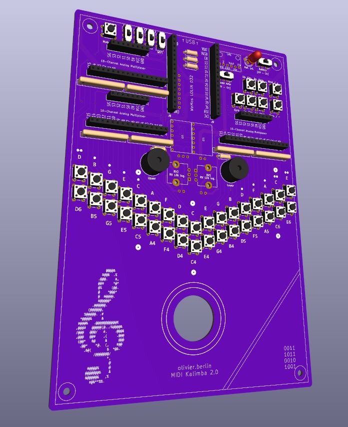
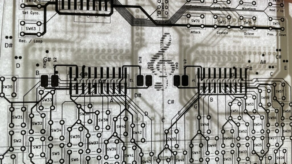
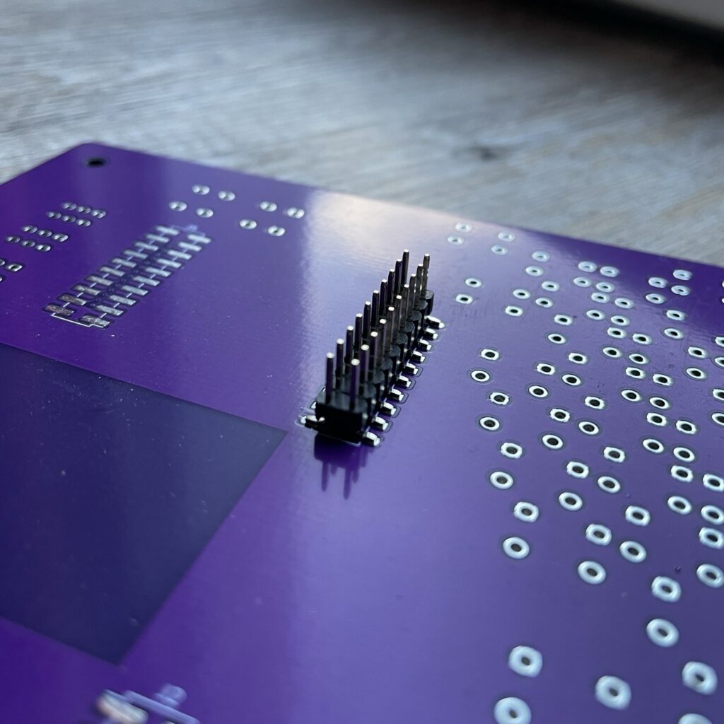
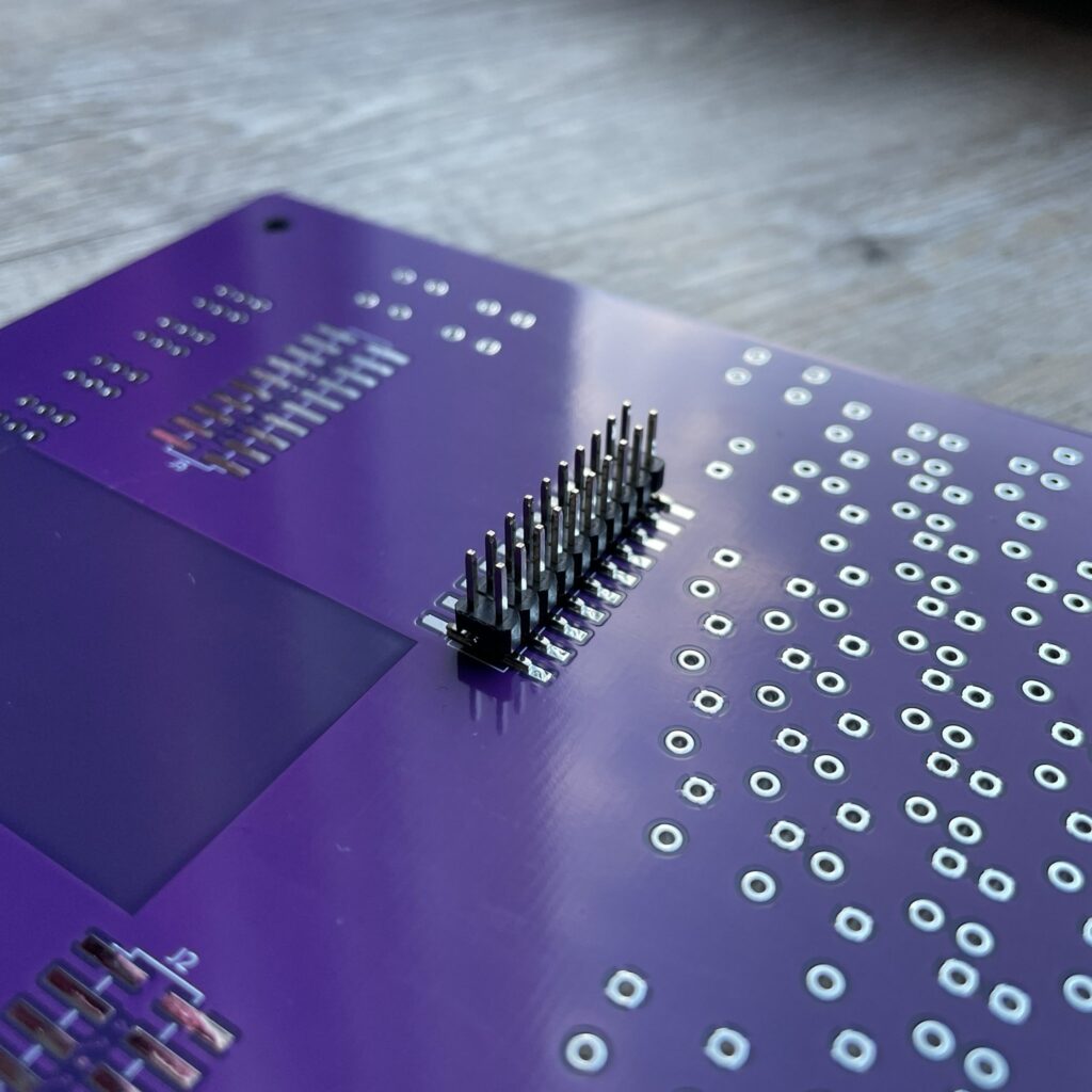
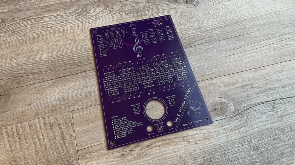
But since I had spent so much time and energy on the V2, just giving up did not sit right with me. I figured that a new approach and some outside the box thinking was necessary. After brainstorming with spare parts I had laying around, the perfect idea came to my mind. I started thinking about adding another PCB to separate buttons / switches to one, and all other electronics components to the second circuit board. This would give me all the necessary space to perfectly arrange my components and achieve a super cleaner look at the same time. In an electronics online shop I found fitting surface mount pin headers and through hole pin sockets could be paired.
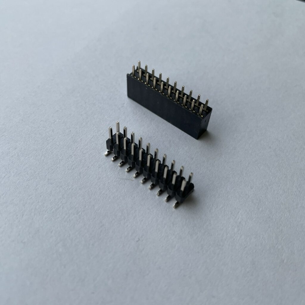
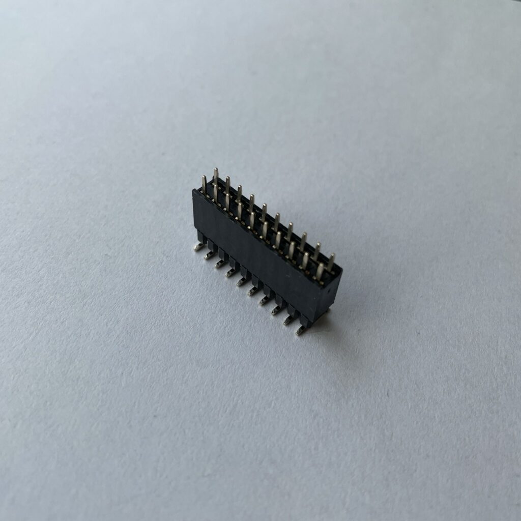
Each connector then provides 20 connections while having a minimal footprint and being mechanically strong. In total, five “2×10” and two “2×4” connectors would provide all the necessary connections between the two PCBs. In total, 116 pins!
The way forward was clear and with the new plentiful PCB space I figured that I could squash another drawback of my first designs (and every regular 17 key Kalimba in general). They can only play the major scale (white keys on a keyboard). This is often fine, but some songs just cannot be played without the non diatonic scale (black keys on a keyboard). I already own one chromatic Kalimba and decided to copy that same layout to add the missing notes to create a chromatic instrument.
This meant more buttons, more multiplexers and more PCB to PCB connections, but was still very much feasible. During the tests on my breadboard, I often used my guitar amp as an output device since it sounds much nicer than those tiny pcb speakers. Another cool thing I started to love was the on board range of effects on my guitar amp that give the sound of this project a whole other dimension. I therefore also decided to add a 3.5 mm audio socket to the bottom PCB as well.
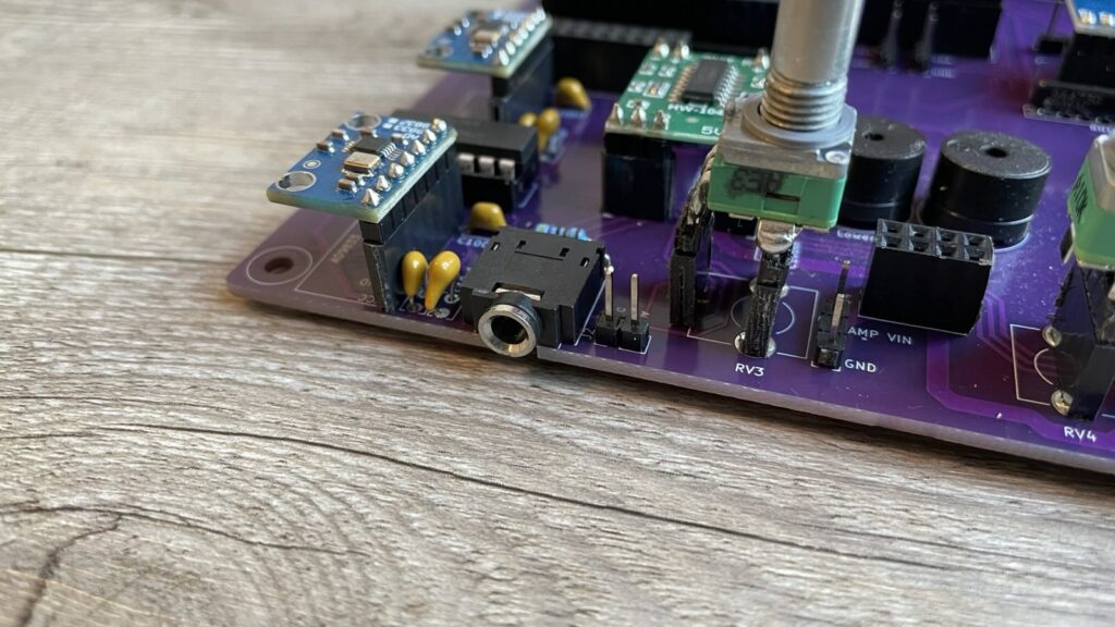
Also, I found the idea interesting to have a gyro on my PCB to be able to modulate the sound using movement in space. Again, a quick test on my breadboard and onto the layout the gyro module went.
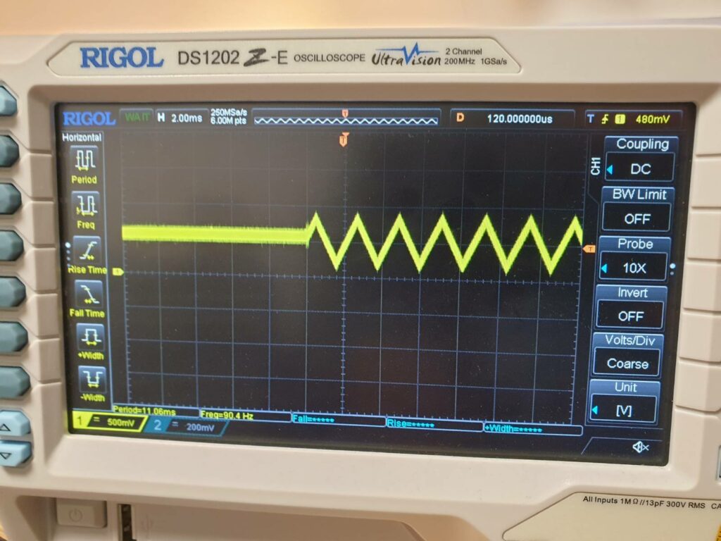
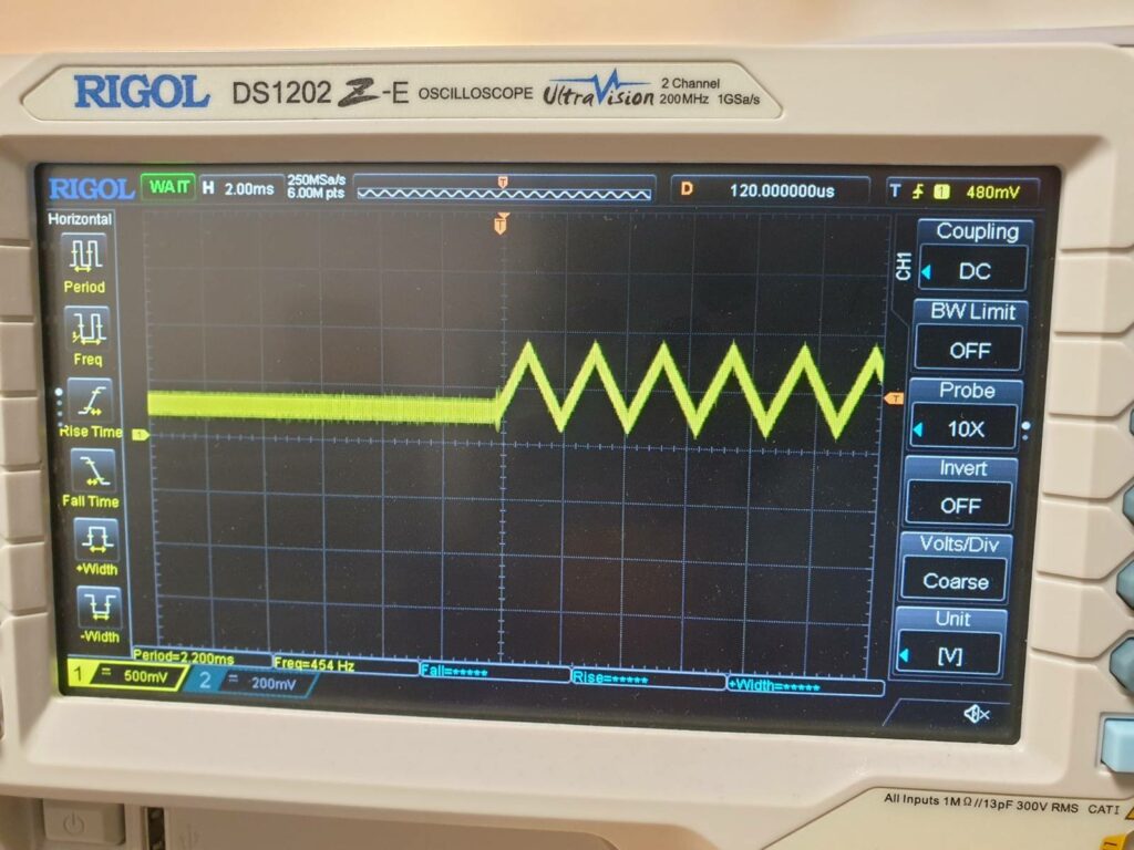
But during the breadboard testing of the complete V3 setup, I found a new thing I was not happy about. The audio generation started and stopped abruptly. This was ok for the tiny PCB speakers, but sounded extremely unpleasant on my guitar amplifier. Every time a note started or stopped playing, a click/pop sound was audible. This was due to the wave not starting from the center but where it last stopped, and from the output volume jumping from 0 to 100 % in an instant.
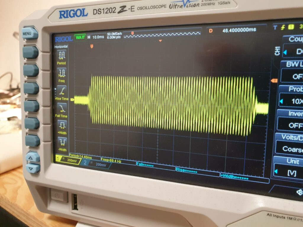
After many tests and lots of help from Rob Tillart (https://github.com/RobTillaart) trying to find the solution within the AD9833 function generators, we decided that a digital potentiometer should be used to neatly fade the audio in and out.
Now the V3 was feature complete and packed. After my learnings from the V2 fail, I again printed both PCB layouts many times, and overlaid the papers against a back lit surface to see if all the mounting points would match and after some more iterations, I arrived at a point where I was unable to detect any more errors. But still during the next couple of evenings, I checked every detail multiple times and always hesitated to click on the order button. I finally gave in and ordered the dual PCB layout. The cost was around 50 € for the complete order.
When the PCBs arrived in the following weeks, I started one of my biggest soldering sessions and was quite let down when the PCBs did not power on at all. There were several more and less severe issues with my design that I still had to figure out. The worst was that the battery switch shorted the battery when the switch was set to the off position. This was also an issue when no battery was connected since it then drained massive amounts of current from the charging circuit (that was then trying to charge GND). But for the battery, this would have meant a complete short circuit when the switch was in the off position. Luckily, I caught the problem before plugging the battery in and therefore did not damage the battery / ESP32 in the process. For this prototype, the issue could be fixed by using my rotary tool to mill a large groove around the battery switch to create an electrically isolated island. The mishap probably happened during a reorganization in the schematics layout editor where pins got connected by accident.
The next big mishap I encountered was the wrong polarity of my battery connector on the PCB. My correct labels showing the order of the colors of the cables made me catch the issue before plugging the battery in. This error was a result of me moving the battery connector from the back side of the PCB V2 to the front side of the bottom PCB V3. To fix this issue on the prototype, I had to create a short custom cable changing the polarity of the battery.
Also I noticed that all the component holes were a bit too narrow to fit my components on the lower PCB. This was because I used pin diameters for pin sockets, which are smaller than actual pins from standard components. It happened due to me assuming the diameters would be the same. There was no real fix to it, apart from mounting all the components on sockets (which I had planned for this prototype anyways).
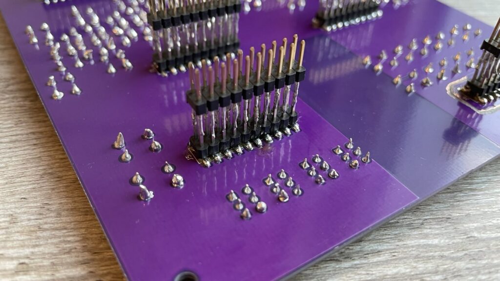
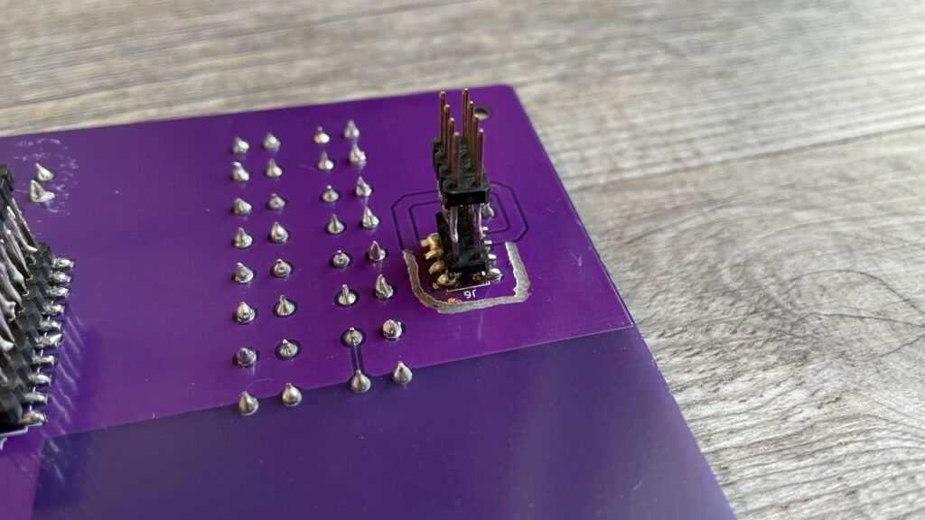
Another major weakness of this version was that the SMD pin headers were hard to solder to the solder pads. Through hole (THT) pin headers were not an option due to me not wanting to have pins and solder sticking out the top PCB towards the player. For this prototype to work, I had to resolder the SMD connectors multiple times and almost every time one or more solder joints broke after taking the instrument apart and mechanically stressing the connection. I even tried a hot air station with lots of solder, only creating a mess in the process and melting my connector. I eventually got all connections working but I knew this was a hard no if anyone would ever want to recreate this project. I therefore opted to create custom solder pads for the SMD headers, that allow for much more solder to be used for each pin, making soldering easy and the connections super sturdy.
With all of these issues identified and fixed on the prototype and in the schematic, the device started to work and with more and more code, the project finally started to come together nicely.
Version 3.1, 3.2 and 3.2.1
For these minor iterations, my goal was to avoid new functionality as best as I can. I just wanted to fix issues and make the assembly as easy as possible.
For the V3.1, the most notable fixes are
- Fixed battery switch to GND issue
- Fixed battery connector polarity issue
- Corrected hole sizes for all the components
- Added a voltage divider before the audio jack to lower output volume
- Removed copper below the ESP32’s antenna for better WiFi reception
- Increased the footprints of the SMD connectors for easier soldering
For the V3.2, the improvements are
- Removal of the added voltage divider of the V3.1 (it did not work as expected)
- Replaced the GND pour of the top PCB with GND traces, to reduce PCB warping and improve WLAN reception.
- Added a switch to select channel to edit settings per channel
- Added more buttons for loop functionality, custom actions, attack …
- Shrinked the solder pads for better bottom PCB GND layer
- Removed the thermal reliefs from bottom PCB GND pins to improve conductivity
For the V3.2.1, the improvements are
- Reset the solder pads size to standard (Made pins unnecessarily hard to solder)
- Readded the thermal reliefs to the GND pins (Made those pins super hard to solder)
- Physically moved the some variable resistors because they were touching the on board audio amplifier
Additional PCBs
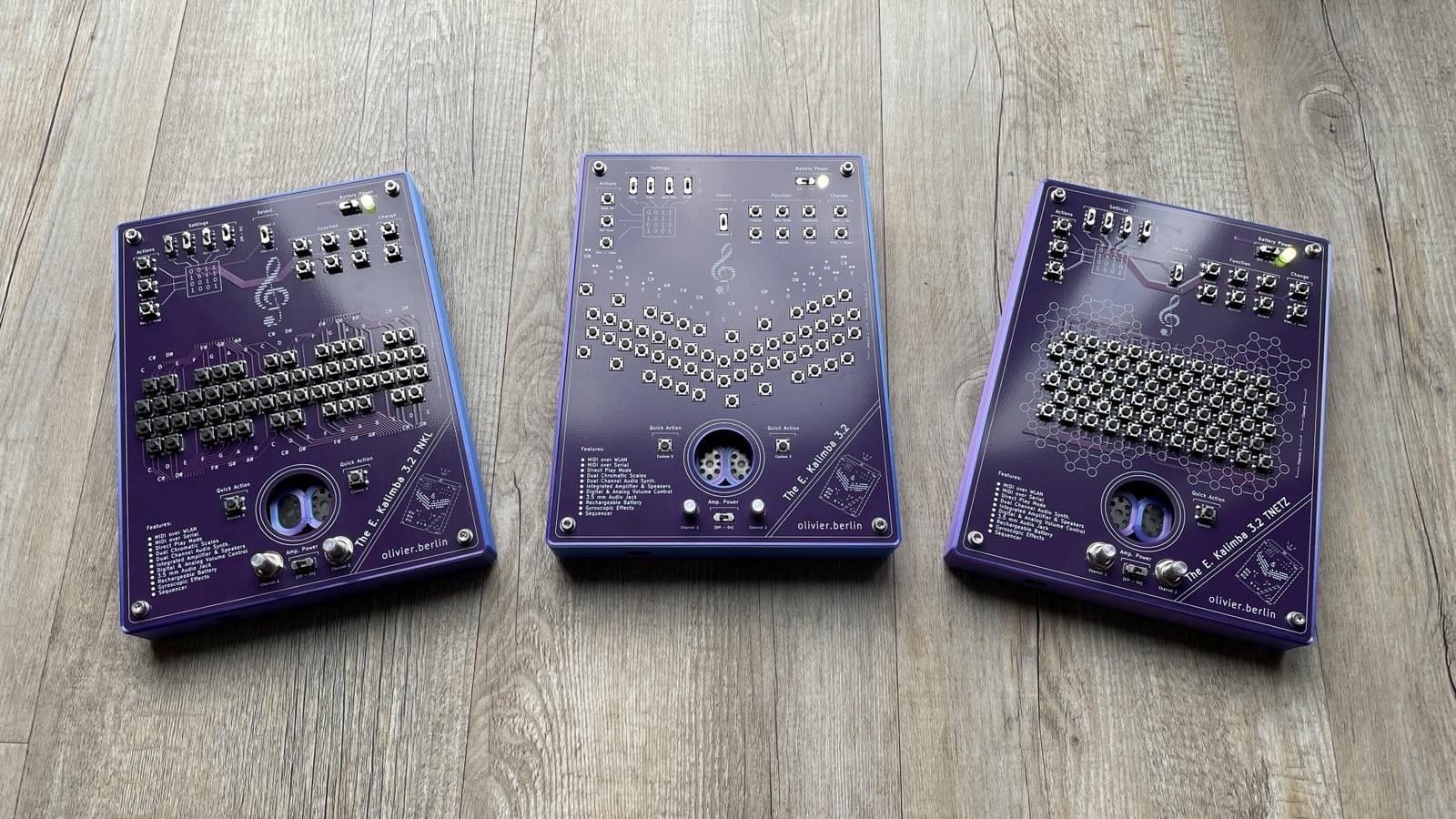
To take advantage of my modular approach, I created and ordered more PCBs to give the project another layer of depth!
Cover
Some feedback I often got was regarding the aesthetics. People did not like that solderpads were visible. I played around with my layout in KiCad and figured I could transform all top PCB components into cutouts, and like that create a cover PCB. JLCPCB warned me that this layout would maybe not machine well, but all PCBs came out perfectly and the resulting visual upgrade of the Electronic Kalimba was absolutely worth it. Only downside, the instrument becomes 8 mm bigger due to the new PCB and the required spacer.
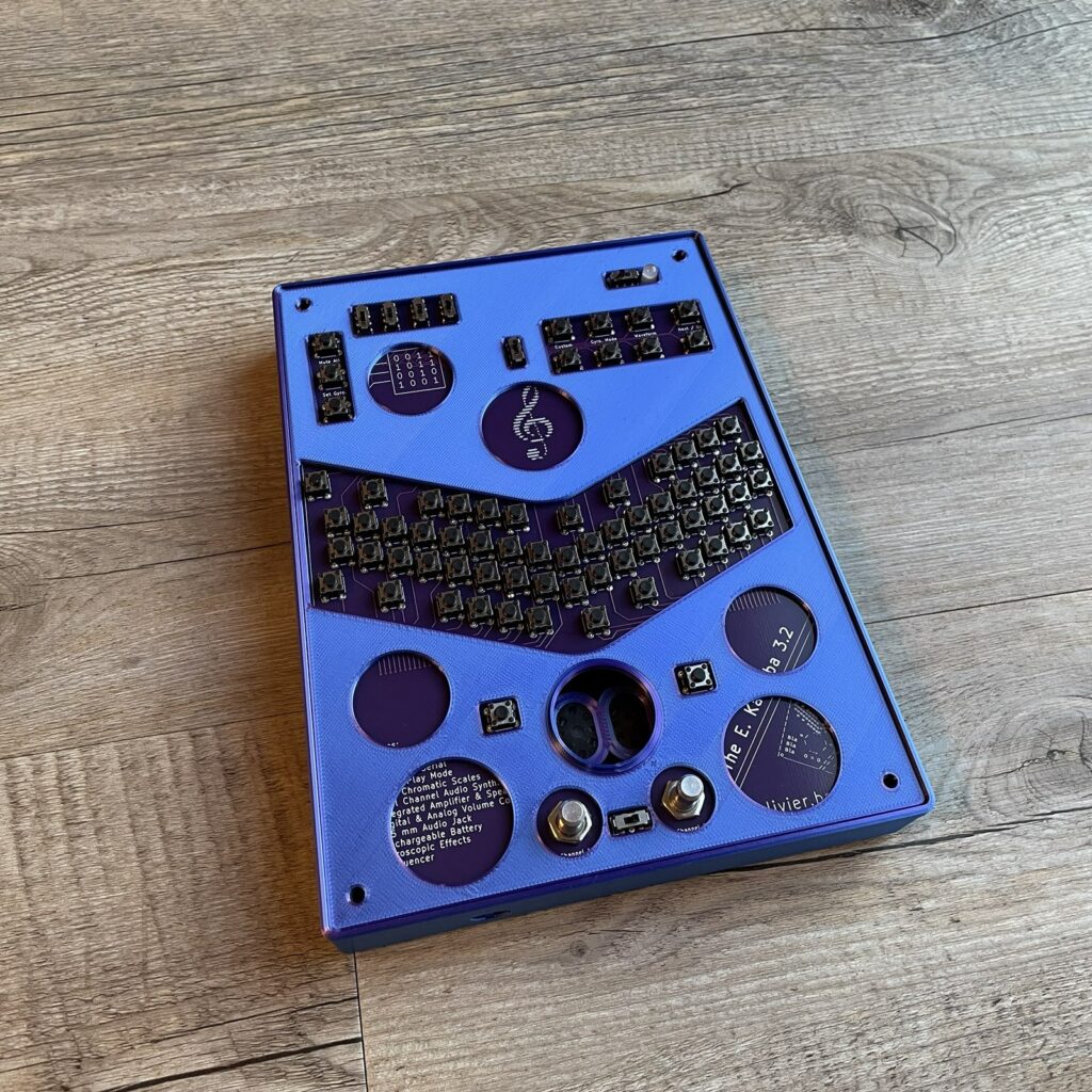
Currently, this top cover only exists for the Kalimba layout, but could easily be created for any other layout as well. The spacer (blue part with cutouts) has as function to make the instrument feel solid, despite the 2 mm gap between the top PCB and the cover PCB.
Keyboard Layout
Other feedback I often received was that the instrument was hard to grasp for non Kalimba players and that I should provide a layout similar to a keyboard. Since the top PCB was meant to be exchangable, this was really easy to design and I ordered one keyboard layout as well.
The required firmware changes were pretty minor, and the resulting instrument is really hard for me to play, since it feels like a Kalimba, but the notes are all in unexpected positions. I don’t know if a Keyboard player could make some music with this, but I am eager to find out.
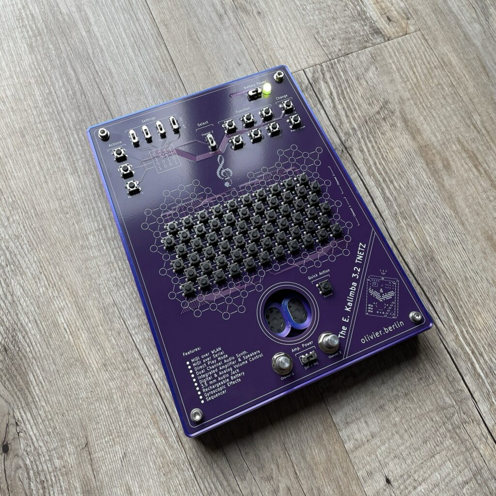
Tonnetz Layout
Another layout that I wanted is the Tonnetz, which was invented by Leonhard Euler in 1739. It is a way to geometrically arrange notes and has some interesting properties. As an example, pressing 3 buttons always results in a perfect chord, and the shape of the pressed buttons determines if it was e.g. a major or a minor chord, or one of many more. With this layout, chords translate into shapes. The only downside, this does not play nicely with the onboard audio generation since it was designed to play two notes at the same time.
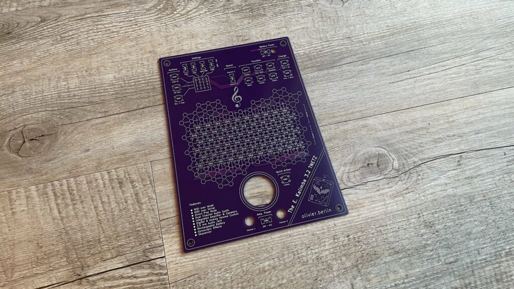
For this layout to function, more in depth firmware changes were necessary. Mainly because the two other designs had as similarity, that Channel 1 and Channel 2 had the same number of notes, and the same layout as well. In this layout, the channels are completely chaotic. However, with some Libreoffice Calc skills, I was able to come up with a mapping that worked at the first try, which I found was astonishing. However, this layout is really easy to play, and also a lot of fun. It is basically a chord machine. Any keypress sounds good. But it is worth noticing that it only really makes sense when used as a MIDI device, since the dual speakers (one for each channel) do not allow for direct playback of full chords… Maybe in a future iteration?
More Top Layouts
I have even more ideas for top layouts, but this project drags on already and I want to start something new, but maybe I’ll come back to the top layouts sometime and create one of these ideas:
- Dual grid layout: Per channel 5 x 5 buttons, the channels arranged left and right
- Circular layout: Similar to Tonnetz, notes can be arranged in circles
- Harmonica layout: When grabbed from behind, the Instrument could be played like a harmonica
- Trumpet layout: Similar to the harmonica layout, a Trumpet layout could be fun to play around with
Many more layouts are possible. Only rule, the SMD pin headers and the PCB outlines cannot be changed. For the rest, possibilities are endless.
Programming
To use the different layouts, a feature flag has been introduced. In one file, the user can now include if the top layout is either Kalimba, Keyboard or Tonnetz. Everything else remains the same, which avoids splitting up the codebase and having to merge changes back and forth. This makes it really easy to switch layouts and test out new things on any of them. However, since I had the spare parts laying around and JLCPCB forces you to always order a set of 5 PCBs anyways, I soldered two more complete bottom PCBs together to have one complete E. Kalimba with each top layout.
Conclusion
This project evolved from a weekend project to my probably most ambitious endeavour so far. With a total of 8 months of work, enormous breadboard setups, 8 custom PCBs that I developed, ordered, soldered and tested, a huge codebase almost using up all of the program memory of my ESP32 and many hard to overcome challenges, I am proud to say that I build something cool. Almost every person that I showed this project so far was impressed. I got good feedback from nerds, musicians and children!
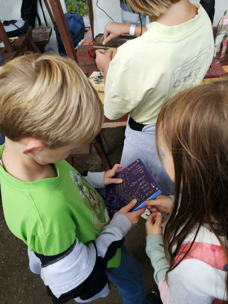
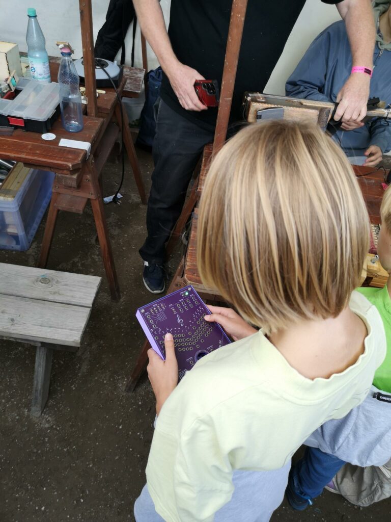
(I asked the parents for their permission to take the pictures)
Overall, the project feels really polished and I use it everyday to play and to experiment with new effects.
If you have an idea for a custom MIDI input device, or an intriguing PCB project feel free to contact me using my email address.